Step – 1 : Define The System Block Diagram
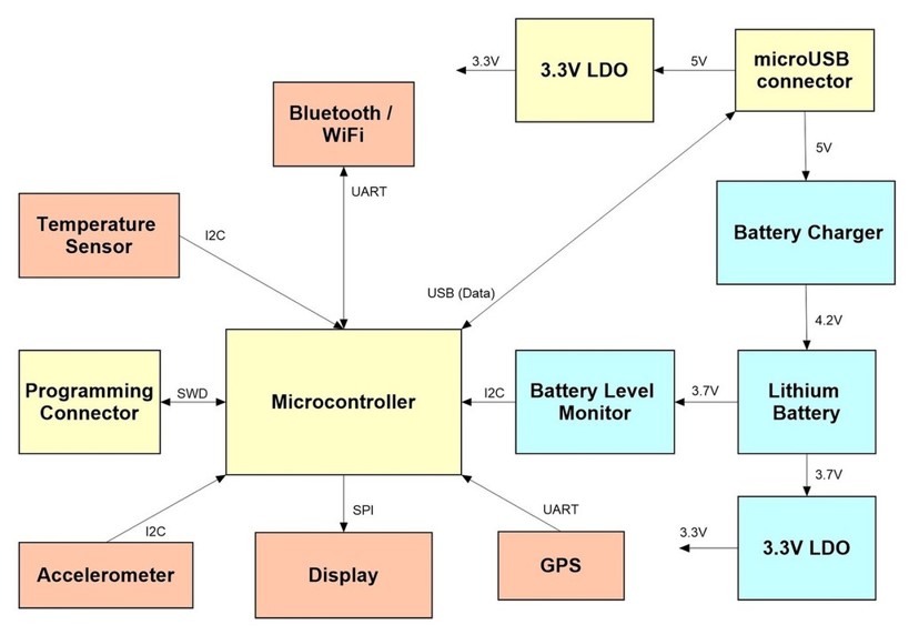
- Start by defining the system-level block diagram. This diagram specifies each electronic function and how all the functional components interconnect.
- Most products require a microcontroller or a microprocessor with various components (displays, sensors, memory, etc.) interfacing with the microcontroller via various serial ports.
- By creating a system block diagram, you can easily identify the type and number of serial ports required. This is an essential first step for selecting the correct microcontroller for your product.
Step – 2: Select Production Component
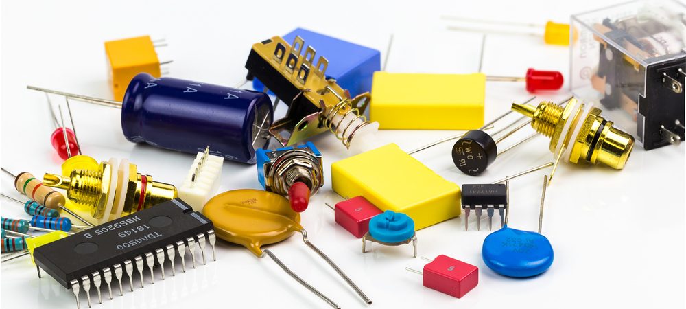
- Select the various production components: microchips, sensors, displays, and connectors based upon the desired functions and target retail price of your product.
- This will allow you to then create a preliminary Bill of Materials (BOM).
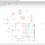
Step – 3: Create The Schematic
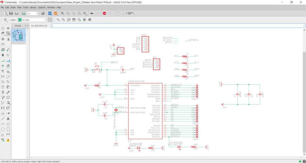
- Design the schematic circuit diagram based upon the system block diagram you created in step 1.
- The schematic provides all the necessary details to build the electronics including how all of the components are connected together.
- A Final Bill of Materials (BOM) will be created detailing every electronic component.
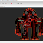
Step – 4: Design The PCB
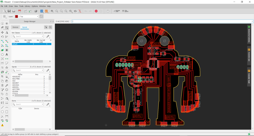
- Design the Printed Circuit Board (PCB), the physical custom designed board that holds and connects all the electronic components.
- Using special software your electronics engineer will turn the abstract schematic (blueprint) into a real-world physical PCB layout.
- This is a complex step because the PCB layout can have a great impact on the performance of the end-product.
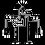
Step-5: Extracting The Board Paths And Outline
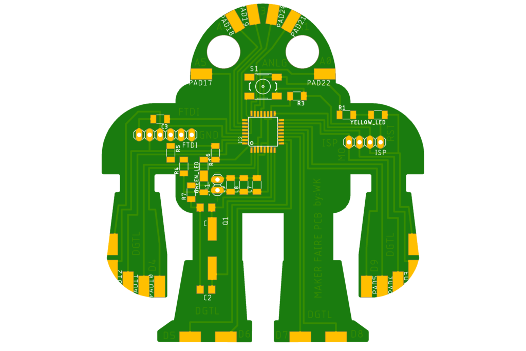
After finalizing the layout of the PCB on Eagle, we want to extract the image that represents the PCB design. To do so we need to follow the following steps.
First we turn off all layers by following the following path “view” > “layer settings” > “select none”
Next we turn on only the layers we want to appear, mainly the ones we need to stay on the copper board during the milling process
Extract the image in a monochrome form
Step-6: Preparing Layout Images
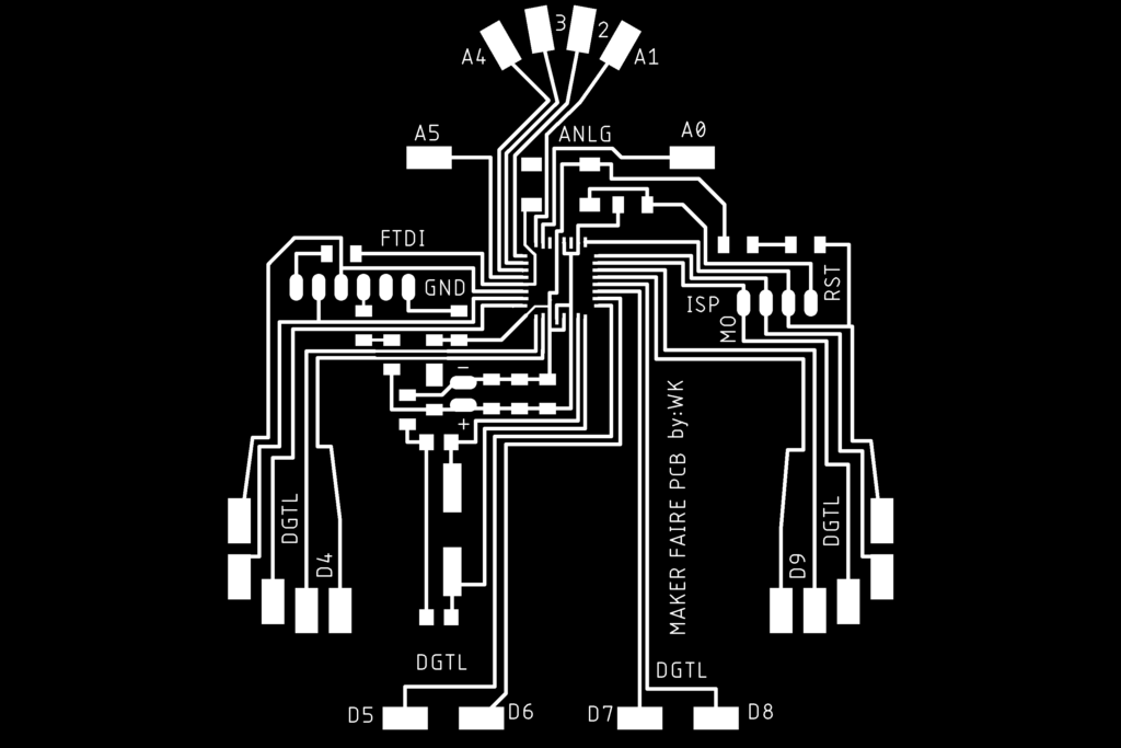
So the next step after extracting the image from Eagle is to produce the images we need to use on Fab Modules to generate the g-code later.
So first we open the original image from Eagle and “extract as” a new copy that you can edit.
Using GIMP is easy, just fill the area you don’t want with black and that’s it. I produced 3 images to be used in fab modules. The images are the following:
- Internal Path represents the internal path of the PCB
- Drilling Positions represents the drilling positions of the PCB
- External Path represents the internal path of the PCB
Please note that in my board, 3 different images needed to be extracted
Step-7: Preparing The G-Code Using Fab Modules
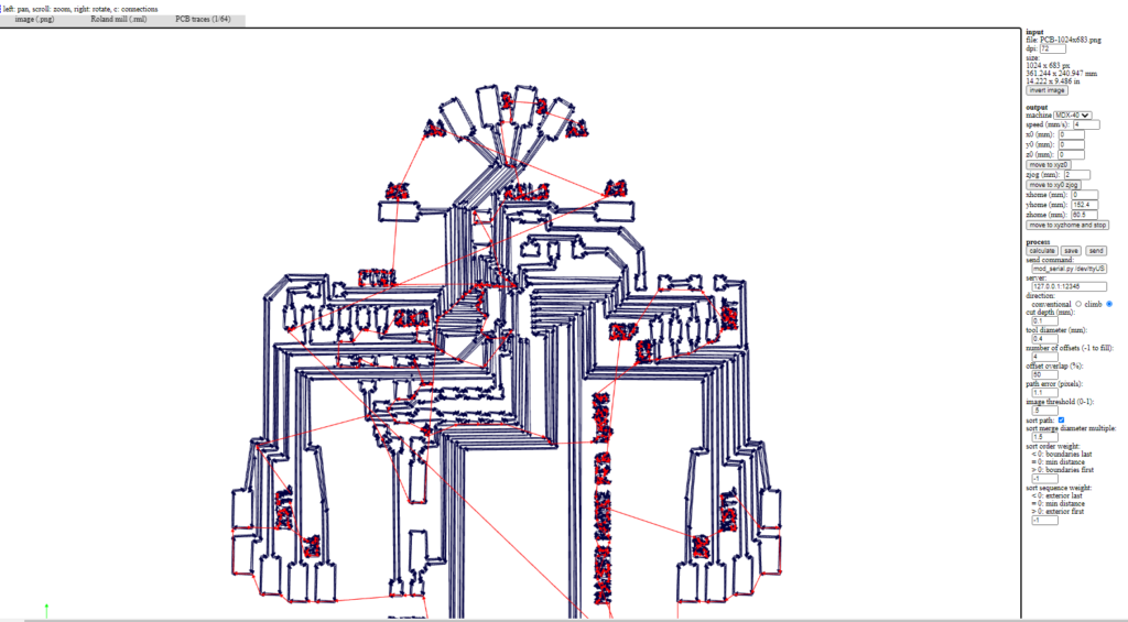
After extracting all images that represent the internal and external paths of the milling bit, it’s time now to produce the g-code. Fab Modules was used to produce the g-code for PCB milling on the Roland MDX-40.
The following steps were followed on Fab Modules to generate the g-code:
- Choose input format and select image (png) that the g-code is going to be generated from
- Select the file from the specific folder
- Go on to Output format and select the format that applies to the CNC machine you are using, in our case it was Roland mill (.rml)
- Then select Process and choose PCB traces (1/64) for internal paths and drilling and PCB Outline (1/32) for the external parameter
- Under Output, select the CNC machine you are using, it was a Roland MDX-40. Change the X0, Y0 and Z0 to save space on copper board used.
- Check the Feed Speed. I was using 4mm/sec for the Internal Traces and 0.5mm/sec to the External Parameter and Drilling
- Adjust the cut depth which should be 0.0 mm for the internal tracing, and 1.7mm for the external parameter and drilling. The tool diameter (milling bit) which was 0.1 mm for the internal traces, 1 mm for the external parameter, and 0.8 mm for drilling. The Number of offsets used was 4. The offset overlap used was 70%. No other adjustments were be made.
- Press the Calculate button
- Finally click the Save button and save it to the designated folder. It would be saved as an .rml file
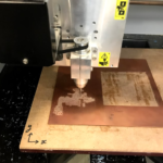
Step-8: Machining The Copper Board
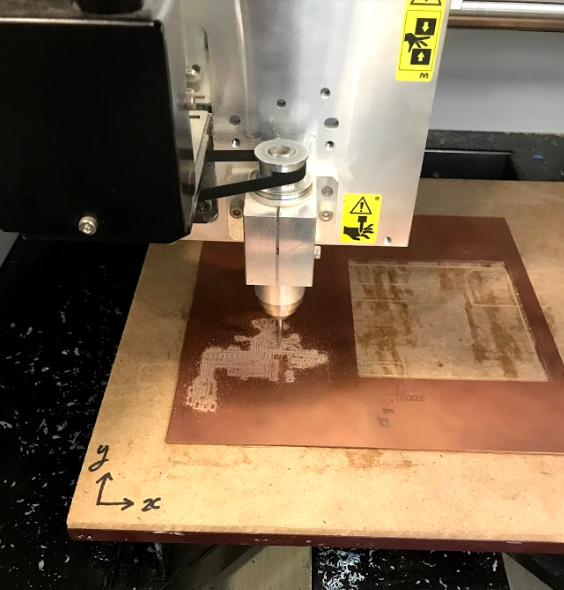
After preparing the G-code, the following steps were taken to mill the layout onto the copper board:
- Drop-Out software was used to send the g-code directly to the Roland MDX-40 to send the .rml file to the CNC machine
- Go to File and select Print Setup
- Choose the name of your printer, in my case it was the Roland TS-30
- Choose RPM. We used was 10,000 for all jobs
- Using Operation Panel set the X and Y-axis on the position where you want your PCB to be engraved on the copper board inside the CNC, then press the XY axis SET butto
- Zero Z-axis at the top surface of the copper board by the help of a multimeter
- Press the Output button. Your CNC machine should now start the process of milling/engraving the copper plate set inside. watch the process until its done
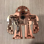
- Check the final result, using a multimeter with the beep setting to make sure components are isolated and all conductivity channels are connected
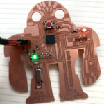
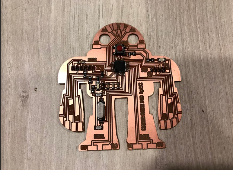
Step-9: Soldering Components
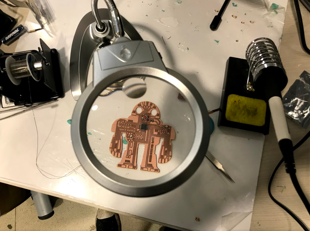
Now that we have the PCB layout cut-out, the next step is to start soldering. In order to do so we first need certain tools to proceed, find the list with specs below:
- Soldering Iron: set at 320 degrees celcius
- Solder wire: 0.5 mm
- Tweezers
- De-soldering copper
- Vacuum
- Tack-it
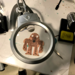
Use a fine tip for the soldering Iron as the components are small, and a magnifying glass would be more than just helpful.
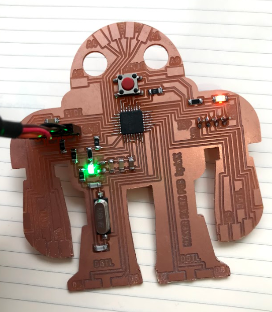
The following list represents the list of components used in My Board:
- ATmega328/P
- 1 x 16 MHz Crystal
- 2 x 22pF Capacitor
- 2 x 10uF Capacitor
- 1 x 1uF Capacitor
- 2 x 100pF Capacitor
- 3 x 10 Kohm Resistor
- 2 x 499 ohm Resistor
- 1 x White LED
- 1 x Green LED
- 1 x 4-pin push button
- 1 x 6-pin FTDI pin headers
- 1 x 6-pin ISP pin headers
- 4 x 6-pin headers
- 1 x 6-pin headers
- 2 x 3-pin headers
- 1 x 4-pin headers
Now for the actual soldering, I used schematic produce by Eagle.
Now for the final step in this process, make sure all connections are ok using the multimeter on the beep option. And you should be set to move on to the next step.
Step-10: Downloading Firmware
After finalizing the code, the next step is to upload the code to the newly constructed Board. To do that, we have to set first the Arduino Board as an ISP. To do so, the following steps are followed.
- Choose the Board as “Arduino/Genuino Uno” by going to “tools” > “board” > “Arduino/Genuino Uno
- Next choose the port where the Arduino is connected
- Then follow the following “file” > “exaples” > “ArduinoISP” to open the Arduino ISP code
- Next upload the code to the Arduino Board
After setting the Arduino board as an ISP, the next step is to push the code to My Board. Connect the Arduino Board to the new Board following those connections:
- 5V to Vcc
- GND to GND
- 10 to Reset
- 11 to MOSI
- 12 to MISO
- 13 to SCK
To do so, the following steps were followed:
- Choose the Arduino/Genuino UNO board
- Choose the terminal that the Arduino is connected to, usually a COM and a Number
- Burn Bootloader by pressing “tools” > “Burn Bootloader”
Now the Board is able to be programmed using the FTDI cable.
Step-11: Evaluate, Program, Debug And Repeat
- Time to evaluate the prototype of the electronics.
- Keep in mind that your first prototype will rarely work perfectly.
- You will most likely go through several iterations before you finalize the design.
- This is when you will identify, debug and fix any issues with your prototype.